Back to Top
Skip to main content
NETL Logo
Harsh-Environment Solid-State Gamma Detector for Down-hole Gas and Oil Exploration
Project Number
DE-FC26-04NT42107
Goal

The goal is to develop a revolutionary solid-state gamma-ray detector suitable for use in harsh environment downhole gas and oil exploration.

Performer(s)

General Electric Global Research Center, Niskayuna, New York 12309

Background

Gamma detection for down-hole gas and oil exploration is used to determine multiple parameters in the assay of possible petroleum bearing formations. Presently this technology is implemented using scintillation detectors consisting of a scintillation crystal, which produces optical photons when excited by a gamma ray, and a photomultiplier tube (PMT), which detects these photons. The detector must withstand the high vibrations and high temperatures present in down-hole applications. Detector performance and service lifetime under high temperature will limit drilling depth as ambient temperatures rise with increasing drill depth. PMT technology can support useful detector lifetimes in the area of 1,000 hours at 150°C, but only 100–200 hours at 175°C.

The temperature limitation of PMT-based technologies represents the most significant economic motivation for developing an alternative detector. This limitation represents a barrier to discovering reserves at greater depths; exploration companies would like to drill deeper while retaining the ability to use the intelligence from gamma detection. The temperature gradient for drilling into the earth is dependent on geographical location and may vary widely, in the range of 8–50° C/1,000 meters.

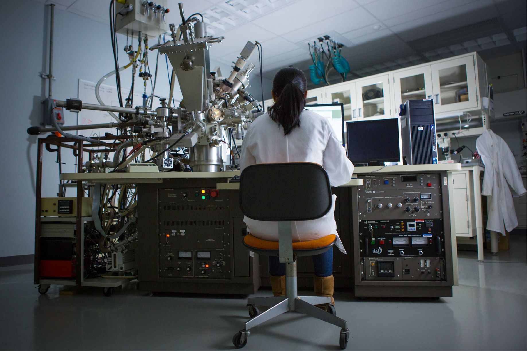
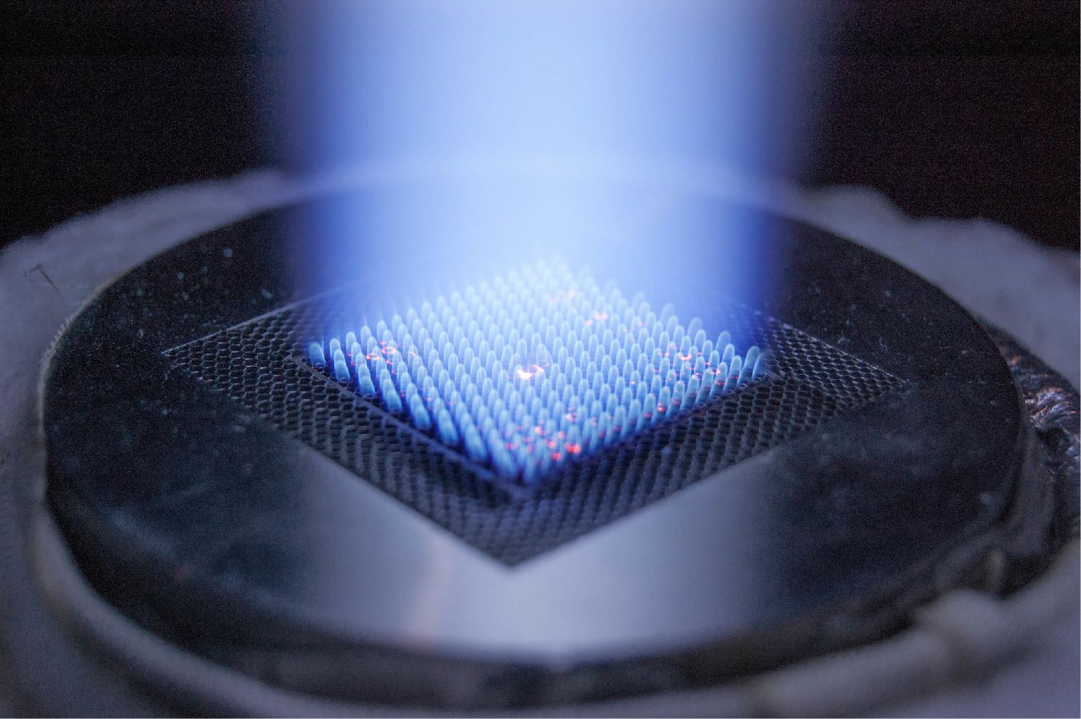
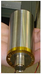
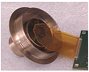
In this project, the GE team will fabricate and characterize the essential elements of an APD/scintillator detector system that can meet the system requirements needed for down-hole applications. The known technical requirements for the APD, scintillator, and detector system will be quantitatively defined. Mathematical models of the detection system will be developed and validated to allow the system response to be estimated from component measurements. A silicon carbide (SiC) APD will be designed, fabricated, and characterized. Scintillator materials will be evaluated for efficiency, emission wavelengths, and temperature stability through phosphor powder screening experiments.

Work during the second phase of the program will include: 1) optimization of the final APD design, 2) growth and characterization of full scintillator crystals of the selected composition, 3) arrangement of the APD device packaging, 4) development of the necessary optical coupling between scintillator and APD, and 5) characterization of the combined elements as a full detector system prepared for commercialization.

Packaged gamma sensor prototype with scintillator end shown at bottom

Results
To date, significant results have been accomplished across a number of tasks. The performers first determined the most critical parameters driving the technical specifications (temperature, reliability and energy resolution). They also refined their system model for estimating performance and evaluating components. Key detector components that have been successfully developed include: avalanche photodiode (APD), scintillator, optical coupler, and electronics. Prototype systems have been developed and tested. The testing showed insufficient system performance to productize the HPHT sensor system at this time. The initial speculation is that the APD electrical leakage was too high and the scintillator crystal's light output was too low resulting in inadequate overall energy resolution. GE will continue to work the optimization of both SiC APDs and the novel scintillator materials through other ongoing GE programs, with the goal of revisiting this system as sufficient improvements are made.

Benefits
The development of a high-temperature, solid-state photodetector fabricated from silicon carbide will circumvent current temperature limitations for gamma detectors as silicon carbide devices can survive and perform at temperatures above 200° C. The new detector will offer two main advantages over current detectors. First, it will be able to operate at higher temperatures, which will allow for deeper drilling and exploration. Second, because the solid-state photodetector has a higher immunity to shock and vibration, it will have a longer life downhole. Both of these advantages will help to reduce the risk and costs for deep drilling.

Summary
The following accomplishments, arranged by general category, have been recorded since the start of the project.

First, the critical parameters driving the technical specifications were determined:

  • System temperature operating capability of 200 – 225° C (for applications)
  • System reliability >1,000 hours at 200°C (for all applications)
  • System energy resolution ~8-9% at room temp, less than 13% at operating temperature (for Density and Spectral applications)

Second, modeling and simulation tools were refined and applied:

  • Refined system model for estimating performance of a given scintillator, avalanche photodiode, and assumptions about coupling optics and packaging.
  • Evaluated several scintillator shapes for optimal light delivery to an APD using optical modeling tools.
Accomplishments (most recent listed first)

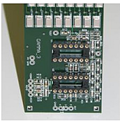
categorized under each of the key detector components, include:

Silicon Carbide Avalanche Photodiode Development

  • Completion of the first iteration 4H SiC separate absorption and multiplication (SAM) region avalanche photodiodes (APD).
  • Generation of detailed fabrication process for the first iteration of SiC APDs. This entailed over 75 steps, documenting processes for metallizations, etching, passivation deposition, wafer cleaning and patterning.
  • Demonstration of ten micron deep etching process in 4H SiC for APD mesa formation using a combination photoresist and metal mask. This included good resolution of features, realization of the desired sloped profile of the sidewall for confinement of the electric field, and demonstration of metallization of cathode (top) and anode (bottom).
  • Demonstration of good quality ohmic contacts to p type SiC for low resistance anode formation.
  • Construction of analytical model to simulate the electric field profile in a SAM structure APD. Initial iteration of APD's designed using this model, yielding a 5 layer epitaxial device, totaling approximately 10 microns in thickness.
  • Completion of device layout variations using CAD program, as used for creation of appropriate photolithography mask sets used in fabrication of the APDs. This design was made flexible such that several device sizes, when fabricated and tested, should elucidate the nature of any significant electrical leakage, e.g. from within the bulk SiC crystal or on the surfaces of the devices.
  • The second iteration of APD’s was completed in September 2005 incorporating modifications as a result of the testing of the APDs from the first iteration.
  • A third generation of SiC APDs was successfully fabricated using an optimized device design. This separate absorption and multiplication region design resulted in significantly reduced dark current, or leakage, particularly near the electric field levels where the device goes into high avalanche.
  • A 4x4 array of SiC APDs was included in the mask set and resulted in many array chips with a common-anode design. These arrays include 16 of the 0.5x0.5 mm die size for an overall active area of about 1.7 mm2.
  • Adapted device simulation models for temperature dependent quantum efficiency and ionization rate behavior in 4H SiC. The newly refined models show excellent agreement with observed results from the third generation APDs. The model will be very useful for future device optimization and subsequent gamma sensor revisions.
  • Measured SiC APDs for dark and photocurrent up to a gain of >100 at temperatures ranging from room temperature to 230 °C. The measurements confirm that on a typical device, the quantum efficiency improves in both magnitude and wavelength shift towards the scintillator output.
  • Measured SiC APDs at room temperature and at 200 °C to show that after 100 cycles of avalanche, the devices retain stable avalanche behavior with no appreciable electrical drift.

Scintillator Development

  • Defined a metric system for evaluating the scintillator powders studied in phase I. The system defined which categories the scintillators would be evaluated for, including a figure of merit on which they could be comparatively judged.
  • Evaluated over 75 scintillator powder candidates for use with the SiC UV APD. Analysis included considerations for light output, wavelength matching to the SiC APD responsivity, stopping power, density, background radiation, manufacturability and temperature dependent light output.
  • Selected best candidate scintillator for crystal growth trials from powder studies. The criteria were based on metrics used to evaluate powders listed above. This met the Phase I goal. The subcontractor has made good progress in developing several crystals for study, however, the crystals were found to absorb heavily in the UV, limiting their applicability. A 'new' material has been identified and growth attempts have been made at GE Global Research. This material outputs in the UV as required. Crystal development will continue with positive crystal measurements.
  • Verified best candidate scintillator material for the high temperature gamma system and acquired a 0.5x0.5 inch cylinder (length and diameter) for the prototype build.
  • Modeled the scintillator and APD combination to determine the optimal properties for the scintillator considering effects from high temperature, various scintillator compositions and activator concentration.

Optical Coupler

  • 11 candidate materials have been identified for use as the optical coupler between the scintillator and the APD array. To date, 9 materials have been tested and results have shown that 1 material failed at sample preparation, 5 failed after 24 hours at 225 °C, 1 failed after 192 hours at 225 °C, and 2 materials continue to show good transmission in the UV and are under continued testing. The remaining 2 materials are either on-order or have just been received.
  • The best candidate optical coupler was selected from the long-term, high temperature testing. The chosen material showed a slight improvement in UV transmission after more than 1,600 hours at over 200 °C. This material, however, also became more rigid, so this will be factored into the gamma sensor prototype design as best possible.

Electronics

  • Four designs of APD amplifier architectures were identified and simulated for signal and noise properties. The simulations factored in APD characteristics expected.
  • The four designs selected were then realized on test circuit boards for lab testing. All designs showed good agreement with simulations suggesting multiple possible approaches for the gamma sensor system.
  • High temperature electronics components have been identified for the eventual construction of a 200 °C amplifier.
  • Power supplies have had initial evaluations and will be further explored for their stability and noise at elevated temperatures.

System Packaging & Prototype Development

  • The APD submount has been design and built using a flex packaging process. This process allows for a user-defined layout of APDs on a desired substrate size and shape. This process also accommodates the placement of singulated detectors for array integration.
  • A second generation sub-mount was built that successfully SiC APDs in the package in both conventional grid-based layouts as well as more aggressive designs where the APDs are placed in a concentric geometry to enhance light collection. Highly reflecting UV films were incorporated in areas not occupied by the detectors to further enhance light collection.
  • A third generation design has been identified that will incorporate electrical connections into the APD sub-mounts to enable the prototype build.
  • The overall high temperature gamma sensor system prototype design is in process, with CAD renderings of all key elements nearly completed.
  • Prototype testing showed insufficient system performance to productize the HPHT sensor system at this time. The initial speculation is that APD electrical leakage is too high as well as the scintillator crystal's light output was too low, with the combined result of inadequate overall energy resolution.
  • On-going programs at GE are studying the optimization of both SiC APDs and our novel scintillator materials with the goal of revisiting this system as sufficient improvements are made.

In addition, the performers consulted with oil well drilling customers to collect “voice of the customer” feedback on how and when the sensor system developed under this program might be best implemented.

Electronics board
Electronics board
Flex electronics attached to APD sub-mount.

Recommendations for Improving Tool Performance
The fact that the SiC APD detector did not detect any gamma radiation can be explained by the fact that the detectable minimum of photoelectrons for the SiC APD arrays was 300, while an actual value of absorbed photons was 12. It is thought that by improving the components of the gamma sensor system, namely the SiC APDs as well as the LaX3 scintillator, would lead to better results,

This program has provided the means to understand the system model, the system design elements that have yielded success in construction as well as the overall approach to detect gammas at 200 °C. With that in mind, there are several approaches proposed in order to improve a performance of the sensor. These may be used in combination to arrive at the energy resolution requirements initially determined in GE’s voice of the customer sessions conducted early on in the program. These include:

  • Use a LaCl3 crystal instead of LaBr3 crystal as a scintillator material to make a batter spectral match of the scintillator crystal's light output and SiC APD response. This will double the number of observable photons to the detector.
  • Use another poly-type of SiC with narrower bandgap (e.g. 3C-SiC) to shift an APD responsivity peak to the longer wavelength range. GE estimations showed that in this case a number of absorbed photons might be increase up to ~50. Note, that a full match of scintillator and APD spectra will give approximately 100 absorbed photons considering an existing design. Thus, additional modification of the system is required to increase a number of collecting photons.
  • Enlargement of a single APD area to 2 mm2 with sixteen devices per array will result in increase in a number of collecting photons above 300. However, this will result in a significant increase in a dark current due to a high defect density in SiC substrates (~104 cm-2) and, thus, a signal-to-noise ratio will be also significantly reduced. In order to provide a leakage current for 2 mm2 APDs with at least the same value as obtained in this project for 0.5 mm APDs, a defect density on SiC substrate must be less than ~6x102 cm-2. CREE Co., (primary supplier of SiC substrates on market) reported recently at an International conference that they have developed 3” 4H-SiC substrates with median dislocation densities of 1.7x102cm-2 (see a slide from CREE presentation in Figure 94). This opens an opportunity to build large area (~2 mm2 ) 4H-SiC APDs with required low leakage currents.
  • Use a modified signal processing circuit by splitting the array into smaller sections and amplifying and shaping the signals from them separately. Implementing multiplication of multiple separate channels (2, 3, 4, 5) probability of the dark counts can be reduced significantly and detection threshold can be reduced to detect weaker signals. Adding one more channel allows increasing sensitivity 2-3 times.
Current Status

(February 2008)
The project is complete. The final report is available below under "Additional Information".

Project Start
Project End
DOE Contribution

$1,319,474 

Performer Contribution

$329,869

Contact Information

NETL – Gary Covatch (gary.covatch@netl.doe.gov or 304-285-4589)
GE Global Research – Peter Sandvik (sandvik@research.ge.com or 518-387-4166)

Additional Information

Final Project Report [PDF-3.40MB]