Business

News and Events
Research and Programs
Business
The goal of this project is to produce a downhole microcomputer system (DMS) capable of operating at 275 °C for 1000 hours. The base DMS will consist of a 68HC11 single chip microcomputer with boot ROM, static RAM, counter/timer unit, parallel input/output (PIO) unit, and serial peripheral interface (SPI) and will also have two peripheral chips, a Data RAM and Mask ROM.
Oklahoma State University, Electrical and Computer Engineering Department, Stillwater, OK 74078
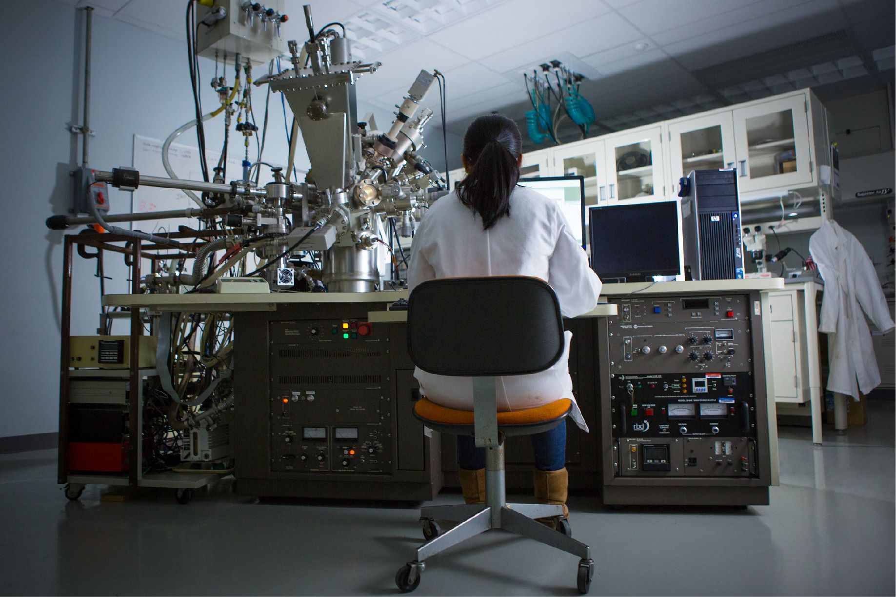
The down-scaling of bulk complementary metal-oxide-semiconductor (CMOS), the dominant integrated circuit (IC) process over the last 4 decades, has increased circuit densities to very high levels and has been the basis for considerable growth in digital signal processing, data acquisition, and intelligent control systems. With down-scaling, however, the CMOS has become increasingly susceptible to failure in high temperature environments. This failure is primarily related to current leakage in transistors in bulk ICs, which becomes catastrophically large at high temperatures.
Wireline and MWD tools are critical electronic components for the energy industry that utilize CMOS technology and PCB designs. Current methods of implementing high temperature circuits drastically increases the costs involved in exploring for hydrocarbons in deep wells. In the case of very high temperature environments (>175°C) it may simply be impossible to implement some electronic control functions or instruments. Dewar flasks and melting materials are being used to keep the internal temperature of the logging tools below 150°C for periods long enough to perform their required measurements, but this is an expensive and temporary solution. The lack of control and measurement circuits for deep well drilling increases the overall risk of successfully reaching the intended target as well as the ability to acquire the data needed to decide on whether or not to complete the well.
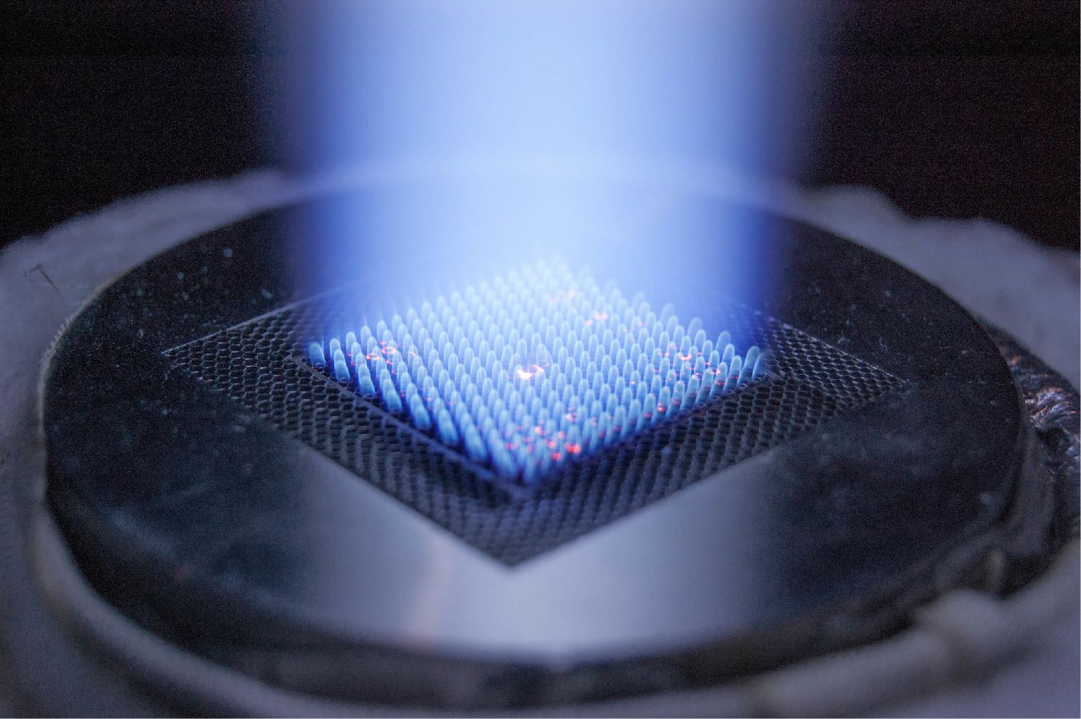
Silica-on-Insulator (SOI) and Silica-on-Sapphire (SOS) are technologies that have greatly reduced the tendency of circuits to suffer leakage at high temperatures. Another emerging technology is Silica Carbon (SiC) circuits. Honeywell Inc., in co-operation with DOE and a joint industry partnership (JIP), is presently working to develop electronic ICs for very high operating temperatures that will utilize SOI technology (see Development of Silicon-on-Insulator (SOI) High Temperature Electronics - DE-FC26-03NT41834).
The proposed SOS-based high temperature electronics will enable reductions in the cost and time for drilling, while making previously unreachable reservoirs producible. OSU’s MSVLSI (Mixed Signal Very Large Scale Integration) group has demonstrated the potential of UltraCMOS at extreme high temperatures for logic, voltage references, analog-to-digital converters and wireless radio frequency (RF) components. This project and the Honeywell JIP project will begin to address the needs of the petroleum industry for HT electronic components with SOI/SOS technology.
Results
The project successfully demonstrated a 275 °C 4K-SRAM and a 275 °C 2K-ROM silicon design with an SPI interface, which are useful for, aerospace, well logging, solar controllers, automobile, and other extreme temperature environment applications. The memory devices results demonstrated proper performance across the frequency, temperature, and voltage corners of 2MHz, 4MHz and 8MHz, 27°C, 200°C, 275°C, and 295°C, and 2.5V, 3V, 3.3V, and 3.6V respectively, making the memory devices suitable for the HC11 chip and other processors, to be used as additional memory storage and/or external system boot memory devices. The SPI SRAM and SPI ROM ‘s 2008 yields are low, but yield and standby power consumption have been significantly improved from the 2007 designs.
Specific results include:
Benefits
The Downhole Microcomputer is a self contained single-chip microcontroller with all the necessary processing and I/O functions located on-chip. Microcontroller functions include read-only memory (ROM) containing application software, random access memory (RAM) for data and variables, counter/timer functions, analog to digital converter (ADC), digital to analog converter (DAC) and one or more of a parallel I/O, asynchronous serial I/O, synchronous or serial I/O. Microcontrollers and/or microcomputers are very important to accurately and efficiently control downhole equipment, communications, data acquisition, and digital signal processing. The DMS will be able to communicate with other components under development in the Deep Trek program. Packaging this capability into a component that can efficiently operate at temperatures of 275oC can greatly extend the exploration and operations of the oil industry to deeper reservoirs with higher temperatures and pressures.
(February 2009)
This project has been completed and the final report is available below under "Additional Information".
$580,704
$146,351
NETL – Gary Covatch (gary.covatch@netl.doe.gov or 304-285-4589
Oklahoma State University – Dr. Chris Hutchens (hutchen@okstate.edu or 405-744-5168)
Final Project Report [PDF-3.42MB]
Pertinent Publications:
Chris Hutchens, Chia-Ming Liu and Hooi Miin Soo, “High temperature Down-hole Microcomputer System, Switched-Mode Power supply Component Development,” GasTIPS, vol. 13, no. 1, 2007.
H. M Soo, Zhe Yuan, R.Sridharan, Vijay Madhuravasal, Dr. C.M. Liu, Srikanth Velore, Jiri Gaisler, Dave Hiscock, Mike Willett, and Dr. C. Hutchens, “Microcontroller with Memory for Extreme Temperature Applications,” HiTEC 2008, Santa Fe, NM, May 12 - 15, 2008.
Hutchens, C., Morris, S. and C. Liu, 2006, A proposed 68HC11 Chip Set for 275 degrees C, IMAPS International Conference on High Temperature Electronics (HITEC 2006), May 15-18, 2006, Santa Fe, New Mexico, U.S.A.