Business

News and Events
Research and Programs
Business
The goal of this project is to develop a downhole switched-mode power supply (SMPS) capable of operating at 275oC for 1000 hours. The base SMPS will include among its necessary components, a V2 controller, Buck Converter, and SiC power switches, which together will constitute a DC-DC SMPS.
Oklahoma State University - Stillwater, Oklahoma 74078
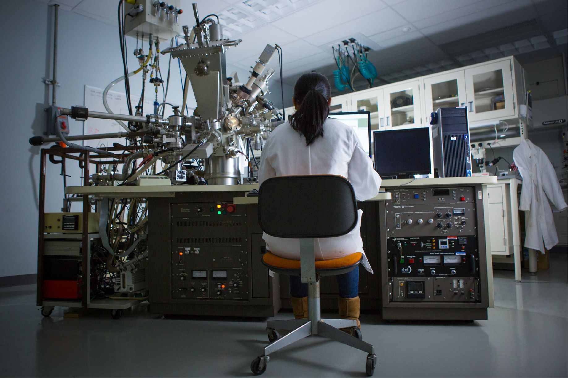
Among the more critical, yet basic, electronic systems needed for extreme temperature subsurface operations is the high efficiency switched mode power supply (SMPS). Such power supplies typically use high frequency switching at frequencies of 50 kHz to 1 MHz to periodically sample and store energy in an inductor, and then convert this stored inductor energy to a charge on a filter capacitor at the desired voltage. Regulation of a SMPS is performed using a control loop to vary the duty cycle of the switch, which regulates the supply output voltage. The use of high frequency switching greatly reduces the size of inductors and filter capacitors in the circuit, and allows for the attainment of power conversion efficiencies up to 95% for high performance multiple output designs. Typical power efficiencies for most SMPS applications are 75% to 90%.
The proposed controller will perform its function in switching power supplies that support downhole measurement systems that heavily rely on digital logic and embedded microcontrollers, e.g., gamma ray counters, frequency based precision pressure and temperature measurement systems, and motor control applications. The proposed controller will be implemented as a monolithic Silicon on Sapphire (SOS) integrated circuit (IC). The SMPS IC will be based on the V2 controller algorithm and use the Peregrine Semiconductor (of San Diego, CA) SOS semiconductor process for fabrication of the IC’s. The Peregrine SOS process is a mature, inexpensive, and stable technology that is well-characterized and similar to the SOI process used by Honeywell in another high temperature electronics project being supported by NETL (NT41834).
For the proposed controller, the following analog building blocks will be developed and packaged: 1) a 7-bit voltage reference, 2) comparators, with and without hysteresis, and 3) a general purpose operational transconductance amplifier (OTA). The development and use of analog building blocks for the V2 mode of control allows their reuse as standard cells or building blocks, further leveraging controller design effort. The architecture of the 275oC SMPS IC will be tailored to support output voltage ranges of 1.5 to 25V and input voltages up to 30V.
This project proposes to formulate a viable low volume solution for packaging IC’s for extreme temperature operation. All parts being considered have either gold metallization or aluminum pads and the Peregrine SOS complementary metal-oxide semiconductor (CMOS) and packages will be aluminum nitride. An aluminum nitride based enclosure will be developed for a SOS V2 controller and the spinoff ICs; comparators, OTAs and voltage reference. The proposed assembly would be in the form of substrates of aluminum nitride with one level sub-mount packaging and a motherboard.
When compared to commercially available SMPS systems, the proposed 275oC SMPS will be unique in three respects: 1) the system will have a very high input to output voltage ratio, 2) at >3 watts, the system will be lower power than typical SMPS systems, and 3) the temperature range of operation will be well beyond existing systems.
Results
Project work began late in 2006. Preliminary overall circuit and high temperature packaging designs have been reviewed by industry advisors. For the first time a room to 275°C switched mode power supply controller integrated circuit has been designed, fabricated, and demonstrated (anecdotal evidence suggest temperatures lower than -50°C are feasible with the present design.) The final buck controller integrated circuit (IC) die is less than 4mm2 and with a final cleanup area should be less than 3mm2 requiring only 5 discrete components to develop a 275°C power supply. The discretes consist of two SiC FET switches, the buck L-C and a small compensation capacitor. A 275°C 5 watt power supply was demonstrated within this task. Greater increments in power are possible incrementally by; 1) changing the voltage level or adding load capacitance, 2) by changing the power switches and increasing the load capacitor, and 3) replacing all components, all with no change to the existing controller IC.
This effort contains many firsts; the first 275°C vee-square (V2) switched mode control IC, first voltage reference IC, first dual comparator IC, first hysteretic comparator IC, all operational beyond 275°C. See Appendix A – Analog blocks datasheets. The first use of SiC “enhancement” mode JFETs in a 275°C application and finally the first fully integrated high side switch circuit for -50 to 275°C operation. All analog cells were developed to implement a 5 watt switch mode power supply demonstration for extreme temperature / harsh environment conditions to 275°C for 1.5 to 28V. Special efforts were made to convert/condition and pad out the analog sub-blocks - voltage reference, operational transconductance amplifier, “NE555”, and comparators. All for use as individual building blocks in future applications. Transformer coupled gate drives and high temperature operable magnetic cores and capacitors suitable for high temperature were identified and tested for use in the design and used in this demonstration. Evaluation of these efforts pointed out two areas in great need of attention for successful 275°C electronics; reliable inexpensive (in relative terms) packaging and high valued i.e. µF, high temperature capacitors. No existing commercial printed circuit boards are suitable for above approximately 240° C applications. SOS CMOS, SiC enhancement JFETs, core inductors and low valued ceramic capacitors proved to be valuable and well suited for the operational temperature range from -50 to 275° C.
A quasi “conventional” ceramic chip packaging of ICs combined with lead carrier type mounting of passive filter components was introduced for hybrid packaging of the complete product. The packaging consisted of an AlN gold motherboard to provide through hole mounting of large components i.e. inductor and input output signals and surface mount area over which a AlN window was AuGe soldered and gold package lead soldered. See Figure 14. The packaging effort proved to be fragile as a result of making the AlN motherboard too thin. The developed SMPS demonstration power supply was demonstrated functional for both 3 and 5 volts at 5 Watt and at room and 275° C. Table 5 presents a summary of the SMPS performance, target specifications and related comments. In the AlN board version overshoot was observed during startup at room temperature suggesting that either the soft start circuit is ramping up too fast or the load capacitor ESR is lower than expected resulting in poor compensation.
Summary
Project work began October 1, 2006, although an Industry Advisory Committee meeting had been held in conjunction with OSU’s 275oC Downhole Microcomputer System project in September. At that time, preliminary overall circuit and high temperature packaging designs were reviewed by the industry advisors, as well as the general utility of the 275oC SMPS. Among the more critical electronic systems needs for extreme temperature subsurface operations, are a high efficiency DC power supply. The key requirements of high efficiency and small size necessitate that it be a switched-mode power supply (SMPS). Such power supplies typically use high frequency switching at frequencies of 50 kHz to 1 MHz to periodically sample and store energy in an inductor, and then convert stored as magnetic energy to charge on a filter capacitor to the desired voltage. Regulation of a SMPS is performed using a feedback control loop to vary the duty cycle of the switch, which regulates the supply output voltage. Moreover, selecting a higher switching frequency greatly reduces the size of inductors and filter capacitors in the circuit, and allows attainment of power conversion efficiencies up to 95% for high performance multiple output voltage designs. Typical power efficiencies for most SMPS applications are 75 to 90%. The objective of this project is to produce a downhole switched-mode power supply (SMPS) capable of operating at 275°C for 1,000 hours, tailored to well logging and MWD applications. However, the resulting solution can be easily modified to satisfy the needs of emerging high temperature electronic systems for the aerospace industry. The base components of SMPS are a V2 controller, Buck Converter, and SiC power switches. These components will be placed in a package capable of operation at 275°C for 1,000 hours.
(January 2009)
This project has been completed and the final report is listed below under "Additional Information".
$465,888
$120,140
NETL – Virginia Weyland (Virginia.weyland@netl.doe.gov or 918/699-2041)
Oklahoma State University – Dr. Chris Hutchens (hutchen@okstate.edu or 405-744-5168)
Publications
Final Report [PDF-3.33MB]
Hutchens, C., Liu, C., Miin Soo, H., and T.C. Grant, 2007, High Temperature Downhole Microcomputer System and Switched-Mode Power Supply Component Development, GasTIPS, vol. 13, no. 1, in press.